Technical Documents
Specifications
Brand
Renesas ElectronicsNumber of Drivers
2
Product Type
LVDS Buffer
Input Type
TTL
Sub Type
Buffer
Output Type
Buffer
Number of Elements per Chip
2
Mount Type
Surface
Package Type
TSSOP
Pin Count
20
Minimum Supply Voltage
3V
Maximum Supply Voltage
3.3V
Minimum Operating Temperature
-40°C
ESD Protection
Yes
Maximum Operating Temperature
85°C
Length
6.6mm
Height
1.05mm
Standards/Approvals
No
Series
9DB102
Automotive Standard
No
Product Details
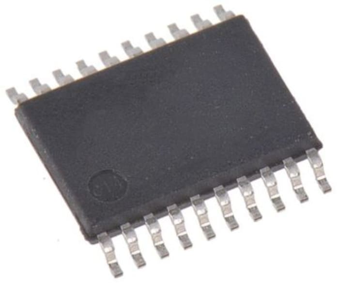
The Renesas Electronics 9DB102 zero-delay buffer supports PCI Express clocking requirements. The 9DB102 is driven by a differential SRC output pair from an IDT CK409/CK410-compliant main clock generator such as the 952601 or 954101. It attenuates jitter on the input clock and has a selectable PLL Band Width to maximize performance in systems with or without Spread- Spectrum clocking.

Ideate. Create. Collaborate
JOIN FOR FREE
No hidden fees!


Stock information temporarily unavailable.
€ 20.75
€ 4.15 Each (In a Pack of 5) (Exc. Vat)
€ 26.04
€ 5.208 Each (In a Pack of 5) (inc. VAT)
Standard
5
€ 20.75
€ 4.15 Each (In a Pack of 5) (Exc. Vat)
€ 26.04
€ 5.208 Each (In a Pack of 5) (inc. VAT)
Stock information temporarily unavailable.
Standard
5
| Quantity | Unit price | Per Pack |
|---|---|---|
| 5 - 5 | € 4.15 | € 20.75 |
| 10 - 20 | € 3.75 | € 18.75 |
| 25 - 95 | € 3.50 | € 17.50 |
| 100 - 245 | € 3.05 | € 15.25 |
| 250+ | € 2.90 | € 14.50 |
Ideate. Create. Collaborate
JOIN FOR FREE
No hidden fees!
Technical Documents
Specifications
Brand
Renesas ElectronicsNumber of Drivers
2
Product Type
LVDS Buffer
Input Type
TTL
Sub Type
Buffer
Output Type
Buffer
Number of Elements per Chip
2
Mount Type
Surface
Package Type
TSSOP
Pin Count
20
Minimum Supply Voltage
3V
Maximum Supply Voltage
3.3V
Minimum Operating Temperature
-40°C
ESD Protection
Yes
Maximum Operating Temperature
85°C
Length
6.6mm
Height
1.05mm
Standards/Approvals
No
Series
9DB102
Automotive Standard
No
Product Details
The Renesas Electronics 9DB102 zero-delay buffer supports PCI Express clocking requirements. The 9DB102 is driven by a differential SRC output pair from an IDT CK409/CK410-compliant main clock generator such as the 952601 or 954101. It attenuates jitter on the input clock and has a selectable PLL Band Width to maximize performance in systems with or without Spread- Spectrum clocking.
Ideate. Create. Collaborate
JOIN FOR FREE
No hidden fees!