Tekninen Dokumentti
Tekniset tiedot
Merkki
Renesas ElectronicsProduct Type
Clock Buffer
Maximum Input Frequency
200MHz
Maximum Propagation Delay Time
350ps
Mount Type
Surface
Package Type
SOIC
Pin Count
8
Minimum Supply Voltage
3V
Maximum Supply Voltage
4.6V
Minimum Operating Temperature
-40°C
Maximum Operating Temperature
85°C
Standards/Approvals
No
Series
IDT23S05E
Automotive Standard
No
Alkuperämaa
Philippines
Tuotetiedot
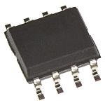
The Renesas Electronics zero delay clock buffer is a high-speed phase-lock loop (PLL) clock buffer, designed to address high-speed clock distribution applications. The zero delay is achieved by aligning the phase between the incoming clock and the output clock, operable within the range of 10 to 200MHz. The PLL feedback is on-chip and is obtained from the CLKOUT pad. In the absence of an input clock, it enters power down.

Ideoi. Luo. Tee yhteistyötä
LIITY ILMAISEKSI
Ei piilokuluja!


Varastotiedot eivät ole tilapäisesti saatavilla.
€ 7,70
€ 0,77 kpl (toimitus putkessa) (ilman ALV)
€ 9,66
€ 0,966 kpl (toimitus putkessa) (Sis ALV:n)
Tuotantopakkaus (Putki)
10
€ 7,70
€ 0,77 kpl (toimitus putkessa) (ilman ALV)
€ 9,66
€ 0,966 kpl (toimitus putkessa) (Sis ALV:n)
Varastotiedot eivät ole tilapäisesti saatavilla.
Tuotantopakkaus (Putki)
10
| Määrä | Yksikköhinta | Per Putki |
|---|---|---|
| 10 - 20 | € 0,77 | € 3,85 |
| 25 - 45 | € 0,73 | € 3,65 |
| 50 - 90 | € 0,714 | € 3,57 |
| 95+ | € 0,702 | € 3,51 |
Ideoi. Luo. Tee yhteistyötä
LIITY ILMAISEKSI
Ei piilokuluja!
Tekninen Dokumentti
Tekniset tiedot
Merkki
Renesas ElectronicsProduct Type
Clock Buffer
Maximum Input Frequency
200MHz
Maximum Propagation Delay Time
350ps
Mount Type
Surface
Package Type
SOIC
Pin Count
8
Minimum Supply Voltage
3V
Maximum Supply Voltage
4.6V
Minimum Operating Temperature
-40°C
Maximum Operating Temperature
85°C
Standards/Approvals
No
Series
IDT23S05E
Automotive Standard
No
Alkuperämaa
Philippines
Tuotetiedot
The Renesas Electronics zero delay clock buffer is a high-speed phase-lock loop (PLL) clock buffer, designed to address high-speed clock distribution applications. The zero delay is achieved by aligning the phase between the incoming clock and the output clock, operable within the range of 10 to 200MHz. The PLL feedback is on-chip and is obtained from the CLKOUT pad. In the absence of an input clock, it enters power down.
Ideoi. Luo. Tee yhteistyötä
LIITY ILMAISEKSI
Ei piilokuluja!